
▦BF CPU
A CPU taped out on real silicon (Tiny Tapeout, GF180MCU) that runs the Brainmess esolang — a multicycle core with no memory of its own, fetching and executing every instruction over an SPI link to off-chip RAM.
Timeline
2026
Team
Joseph Wan & Joseph Mensah
Role
RTL design & verification
Skills
Silicon, Verilog, CPU
Built with
LONG STORY SHORT
I taped out a real chip that runs Brainmess — a CPU with no memory of its own, reaching every byte of program and data over SPI.
Brainmess is a minimal, Turing-complete language with exactly eight instructions: > < move a data pointer, + - change the cell under it, . , do output and input, and [ ] form loops. It's small enough to build in hardware and complete enough that doing so means building a real CPU — a fetch/decode/execute machine with a program counter, a data pointer, and control flow.
So that's what this is: a multicycle Brainmess CPU, written in Verilog, run through the open-source ASIC flow, and manufactured as a 1×1 Tiny Tapeout tile on the GF180MCU process. It is a physical chip that runs programs.
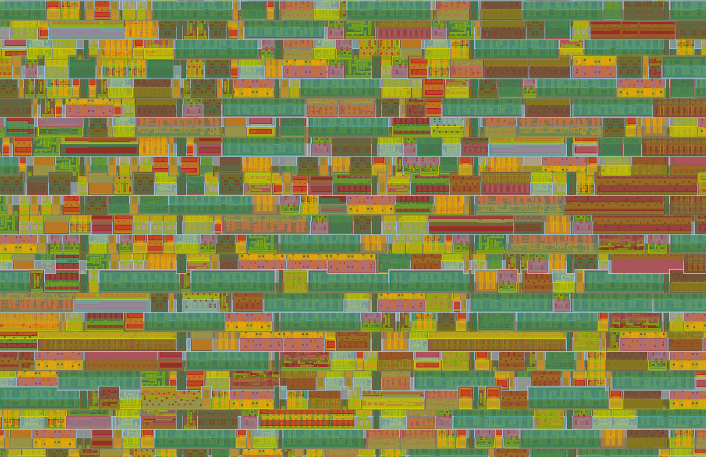
What the chip looks like up close
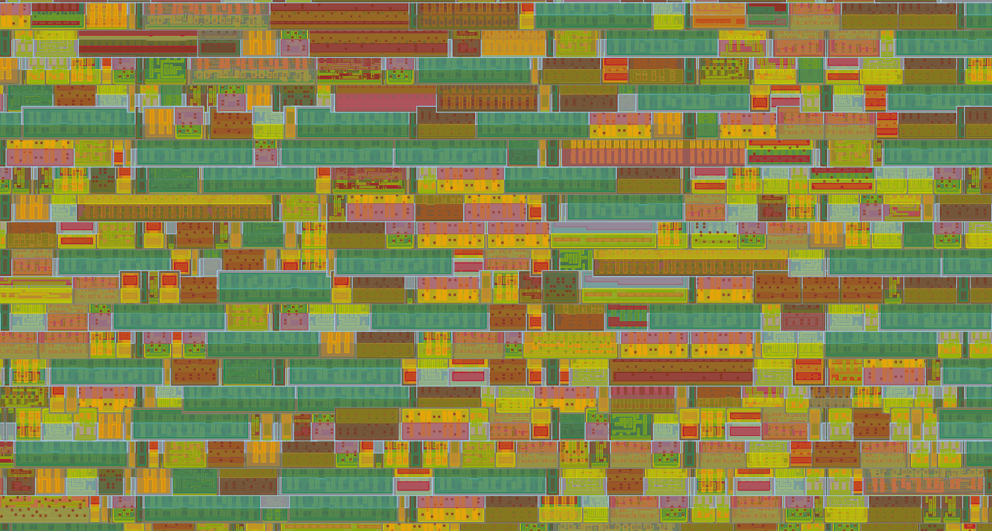
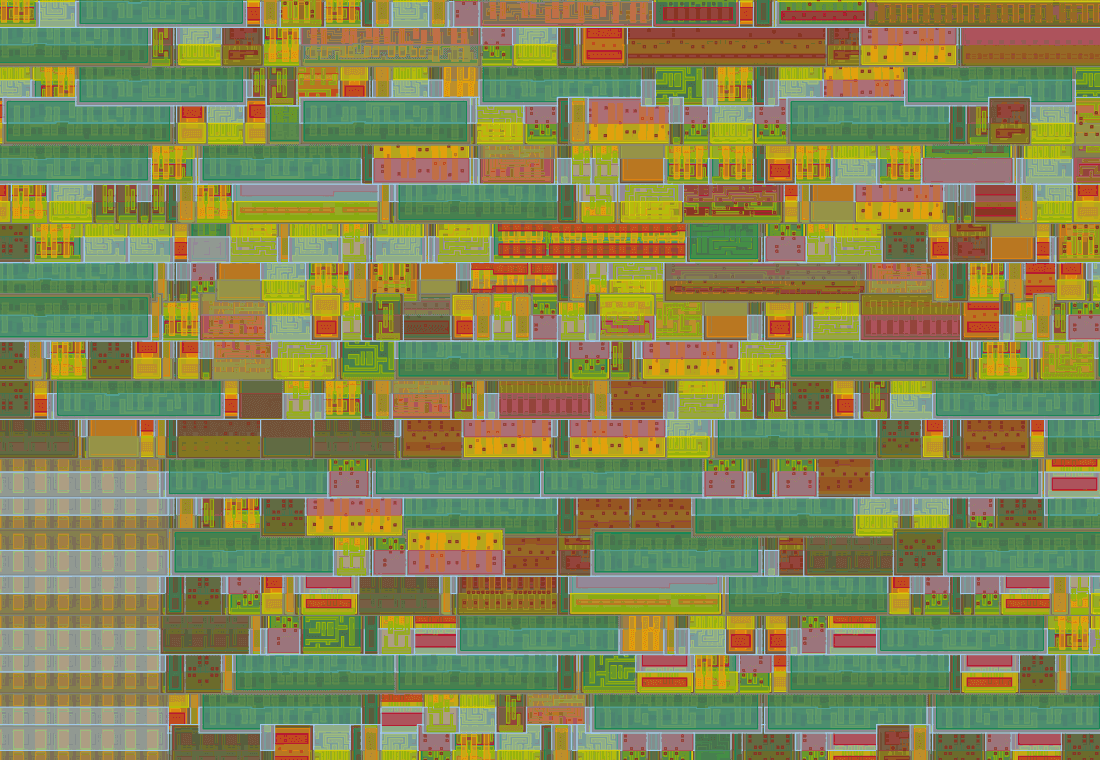
The full GDS render is beautiful, but the useful detail is easier to see when you zoom in. The repeated green horizontal bands are standard-cell rows; the brighter yellow, orange, red, and blue shapes are routed layers and vias tying the cells together. This is the point where the project stops being a Verilog file and becomes geometry the foundry can manufacture.
That density is also why the architecture has to stay simple. There is no room to casually add large memories or wide datapaths, so the design leans into a small control core, a narrow byte datapath, and an external-memory protocol.
How it works
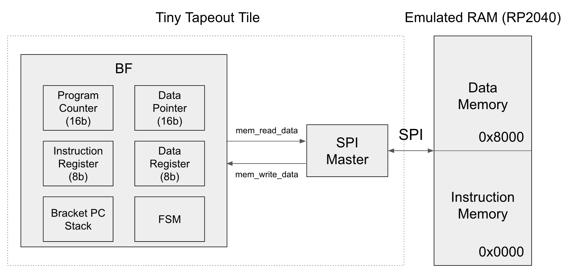
The core is a ten-state FSM — fetch, decode, the read/modify/write states for + -, the I/O states for . ,, and forward/backward scan states for loops — around a program counter and data pointer (both 16-bit) and 8-bit instruction and data registers. Loops are the interesting part: a small 6-deep hardware stack remembers the address of each open [, so a matching ] jumps back in one step; nesting deeper than the stack falls back to scanning the program for the matching bracket, so correctness never depends on the stack being big enough.
On-chip core
BF
- 10-state multicycle FSM
- PC + data pointer (16b)
- 6-deep bracket stack
On-chip bridge
SPI master
- 32-bit command frames
- 0x03 read / 0x02 write
- one transaction per access
Off-chip
RP2040 SPI RAM
- 64 KB, 23LC512 emulation
- instructions 0x0000–0x7FFF
- data tape 0x8000–0xFFFF
Fast path
A six-entry hardware stack remembers recent loop-open PCs.
Correctness path
If nesting is deeper, the FSM scans forward or backward to find the matching bracket.
No memory of its own
The defining constraint: the chip has no on-chip RAM. Both the program and the data tape live off-chip in an RP2040 running Michael Bell's spi-ram-emu, which impersonates a 23LC512 — SPI mode 0, 0x03 to read, 0x02 to write, 16-bit addresses. A single 16-bit space is split in half: 0x0000–0x7FFF holds instructions, 0x8000–0xFFFF is the data tape.
Everything the core does therefore travels as an SPI transaction. An on-chip SPI master serialises each request into a 32-bit command/address/data frame and shifts it out MSB-first. Fetching an instruction is one read; . and , are one transfer each; and + or - is a read-modify-write — two transactions to touch a single cell.
0x0000-0x7FFF
Instruction memory
BF opcodes are fetched from the low half of the off-chip RAM.
0x8000-0xFFFF
Data tape
The data pointer walks byte cells in the high half of memory.
One instruction's journey
Because memory is remote, a single instruction is a little pipeline of bus traffic rather than a one-cycle affair — the FSM walks it through fetch, decode, and, for the arithmetic ops, a full read-modify-write against the tape before advancing.
- 1
Fetch
instr over SPI
- 2
Decode
one of 8 ops
- 3
Read cell
SPI read at DP
- 4
Modify
+ / − / I/O
- 5
Write cell
SPI write back
- 6
Advance
PC++ or jump
CMD
0x03 / 0x02
ADDR[15:8]
high byte
ADDR[7:0]
low byte
DATA
8 bits
The pins
A Tiny Tapeout tile gives you eight dedicated inputs, eight outputs, and eight bidirectional pins — and this design uses all of them. The input and output bytes map straight onto Brainmess's , and .; the bidirectional pins carry the SPI link to memory plus a small handshake so the host can feed input, latch output, and start the machine.
ui[7:0]
The input byte the , instruction reads.
8 dedicated input pins
uo[7:0]
The output byte the . instruction writes.
8 dedicated output pins
uio[0:3]
SPI master out to the off-chip RAM.
CS · MOSI · MISO · SCK
uio[4:7]
Host I/O handshake and run control.
start · out_valid · in_valid · in_ack
Verifying a chip you can't probe
Silicon is unforgiving: once a design is taped out, there is no patch. So the design is tested at three levels before it ever becomes layout — the SPI master on its own, the BF core against a fake memory, and the whole chip against a mock SPI RAM, each with cocotb testbenches.
The SPI master
Driven against a mock SPI RAM, checking every frame — command, address, data, and timing.
Makefile.spi · cocotb
The BF core, isolated
The FSM run against a fake memory, verifying each instruction and nested-loop behaviour.
Makefile.bf · cocotb
The whole chip
The full design against a mock SPI RAM, end to end — real programs, real output.
Makefile.top · cocotb
From RTL to silicon
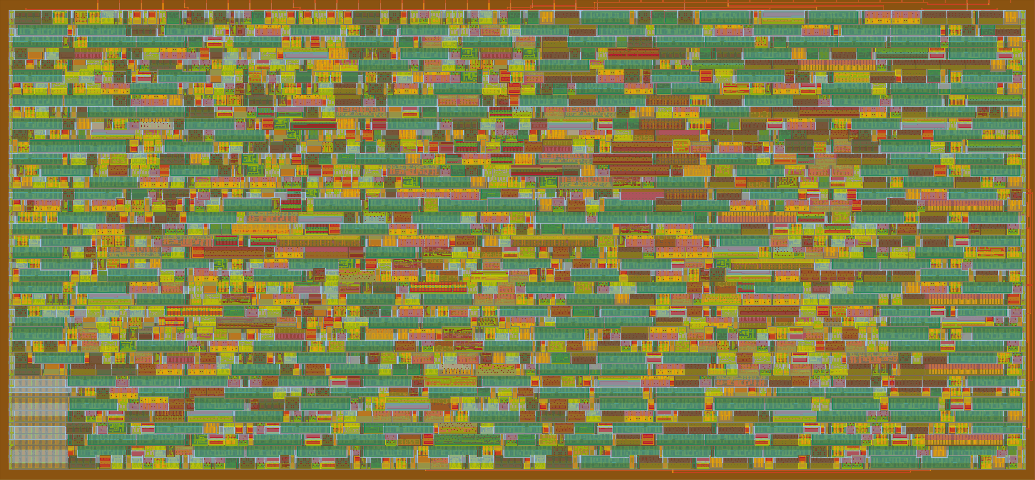
The Verilog runs through the open-source hardening flow and comes out as a placed-and-routed layout: standard cells packed into rows, wired across metal layers, dropped into one Tiny Tapeout tile. The image is the actual gds_render of this project — and it's explorable in 3D through the Tiny Tapeout GDS viewer linked above.
It's one thing to simulate a CPU; it's another to hold the constraint that there is no memory here and design a machine that works anyway by talking to the world one SPI frame at a time.
What comes next
The physical chip is expected later this fall, packaged and ready for bring-up. That is the part I am most excited for now: taking the design past simulation and layout, wiring it into the real Tiny Tapeout board environment, and proving that the packaged silicon behaves like the RTL said it would.
The next step is full post-silicon validation — loading real BF programs, exercising the SPI RAM path, checking the input/output handshake, and comparing observed behavior against the cocotb tests that shaped the design. I am looking forward to that process because it is where the project becomes more than "the build passed": it becomes a chance to learn how real chips are powered up, measured, debugged, and trusted.
Why I built it this way
- A real CPU, not a toy. Brainmess's eight instructions still demand a program counter, a data pointer, control flow and I/O — the whole fetch/decode/execute loop, in hardware.
- Own the memory constraint. No on-chip RAM forced a clean split: a core that computes, and an SPI master that fetches — every access an explicit transaction.
- Loops in hardware, with a fallback. A 6-deep bracket stack makes common nesting O(1), while a scan path keeps arbitrarily deep programs correct.
- Prove it before it's permanent. Three levels of cocotb tests — bus, core, and full chip — because you cannot debug a chip after it ships.
NEXT UP …